- 您现在的位置:买卖IC网 > Sheet目录985 > ISL29020IROZ-EVALZ (Intersil)EVALUATION BOARD FOR ISL29020
�� �
�
�ISL29020�
�.�
�BITS� 3:2�
�0:0�
�0:1�
�1:0�
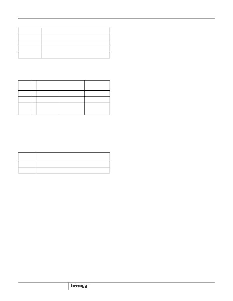
�TABLE� 7.� RESOLUTION/WIDTH�
�NUMBER� OF� CLOCK� CYCLES�
�2� 16� =� 65,536�
�2� 12� =� 4,096�
�2� 8� =� 256�
�Here,� n� =� 4,� 8,� 12� or� 16.� This� is� the� number� of� ADC� bits�
�programmed� in� the� command� register.� 2� n� represents� the�
�maximum� number� of� counts� possible� from� the� ADC� output� in�
�Internal-Timing� mode.� Data� is� the� ADC� output� stored� in� the�
�data� registers� (01� hex� and� 02� hex).�
�EXTERNAL� TIMING� MODE�
�E� =� ---------------------------� � DATA�
�1:1�
�2� 4� =� 16�
�Range� (� k� )�
�Timer�
�(EQ.� 4)�
�5.� Range:� Bits� 1� and� 0.� The� Full� Scale� Range� (FSR)� can� be�
�adjusted� via� I� 2� C� using� Bits� 1� and� 0.� Table� 8� lists� the�
�possible� values� of� FSR� for� the� 500k� Ω� R� EXT� resistor.�
�TABLE� 8.� RANGE/FSR� LUX�
�Here,� Timer� sets� up� the� ADC’s� maximum� count� reading� and�
�it� is� the� number� of� clock� cycles� accrued� in� the� integration�
�time� (set� by� sync_I� 2� C� pulses)� in� External-Timing� mode.� It� is�
�stored� in� the� data� registers� 01h� and� 02h� when� the� command�
�BITS�
�1:0�
�0:0�
�0:1�
�1:0�
�1:1�
�k�
�1�
�2�
�3�
�4�
�RANGE(k)�
�Range1�
�Range2�
�Range3�
�Range4�
�FSR� (LUX)� @�
�ALS� SENSING�
�1,000�
�4,000�
�16,000�
�64,000�
�FSR� (LUX)� @� IR�
�SENSING�
�����is� coded� as� 1xx101xx.� Data� is� the� ADC� output.� In� this� mode,�
�the� command� has� to� be� sent� out� again� with� code� 1xx100xx�
�to� request� the� ADC� output� data� from� registers� 01h� and� 02h.�
�External� Scaling� Resistor� R� EXT� for� f� OSC� and�
�Range�
�The� ISL29020� uses� an� external� resistor� R� EXT� to� fix� its�
�internal� oscillator� frequency,� f� OSC� and� the� light� sensing�
�Data� Registers� (01� hex� and� 02� hex)�
�The� device� has� two� 8-bit� read-only� registers� to� hold� a� 16-bit�
�range,� Range.� f� OSC� and� Range� are� inversely� proportional� to�
�R� EXT� .� For� user� simplicity,� the� proportionality� constant� is�
�referenced� to� 500k� Ω� :�
�Range� =� ------------------� � Range� (� k� )�
�f� OSC� =� ------------------� � 725� kHz�
�data� from� ADC� or� Timer.� The� most� significant� byte� is�
�accessed� at� 02� hex,� and� the� least� significant� byte� is�
�accessed� at� 01� hex.� The� registers� are� refreshed� after� every�
�conversion� cycle.�
�500k� Ω�
�R� EXT�
�500k� Ω�
�R� EXT�
�(EQ.� 5)�
�(EQ.� 6)�
�ADDRESS�
�(hex)�
�01�
�02�
�TABLE� 9.� DATA� REGISTERS�
�CONTENTS�
�Least-significant� byte� of� most� recent� ADC� or� Timer� data.�
�Most-significant� byte� of� most� recent� ADC� or� Timer� data.�
�Integration� Time� or� Conversion� Time�
�Integration� time� is� the� period� during� which� the� device’s�
�analog-to-digital� ADC� converter� samples� the� photodiode�
�current� signal� for� a� measurement.� Integration� time,� in� other�
�words,� is� the� time� to� complete� the� conversion� of� analog�
�photodiode� current� into� a� digital� signal� (number� of� counts).�
�Calculating� Lux�
�The� ISL29020’s� ADC� output� codes,� DATA,� are� directly�
�proportional� to� lux� in� the� ambient� light� sensing,� as� shown� in�
�Equation� 1.�
�Integration� time� affects� the� measurement� resolution.� For�
�better� resolution,� use� a� longer� integration� time.� For� short� and�
�fast� conversions,� use� a� shorter� integration� time.�
�E� cal� =� α� ×� DATA�
�(EQ.� 1)�
�The� ISL29020� offers� user� flexibility� in� the� integration� time� to�
�balance� resolution,� speed� and� noise� rejection.� Integration� time�
�Range� (� k� )�
�R� EXT�
�1�
�(EQ.� 7)�
�t� int� =� 2� � --------------� =� 2� � ----------------------------------------------�
�f� OSC�
�Here,� E� cal� is� the� calculated� lux� reading.� The� constant� α� is�
�determined� by� the� Full� Scale� Range� and� the� ADC’s�
�maximum� output� counts.� The� constant� can� also� be� viewed�
�as� the� sensitivity:� the� smallest� lux� measurement� the� device�
�can� measure,� as� shown� in� Equation� 2.�
�(EQ.� 2)�
�α� =� ----------------------------�
�Count� max�
�Here,� Range(k)� is� defined� in� Table� 8.� Count� max� is� the�
�can� be� set� internally� or� externally� by� programming� the� bit� 4� of�
�the� command� register� 00(hex).�
�INTEGRATION� TIME� IN� INTERNAL-TIMING� MODE�
�Most� applications� will� use� the� Internal-Timing� mode.� In� this�
�mode,� f� OSC� and� ADC� n-bits� resolution� determine� the�
�integration� time,� t� int,� as� shown� in� Equation� 7.�
�n� n�
�725kHz� ×� 500k� Ω�
�maximum� output� counts� from� the� ADC.�
�where� n� is� the� number� of� bits� of� resolution� and� n� =� 4,� 8,� 12� or�
�The� transfer� function� used� for� each� timing� mode� becomes:�
�INTERNAL� TIMING� MODE�
�16.� 2� n� ,� therefore,� is� the� number� of� clock� cycles.� n� can� be�
�programmed� at� the� command� register� 00(hex)� bits� 3� and� 2.�
�E� =� ---------------------------� � DATA�
�Range� (� k� )�
�n�
�2�
�6�
�(EQ.� 3)�
�FN6505.1�
�August� 20,� 2009�
�发布紧急采购,3分钟左右您将得到回复。
相关PDF资料
ISL29021IROZ-EVALZ
EVAL BOARD FOR ISL29021IROZ
ISL29023IROZ-EVALZ
EVALUATION BOARD ISL29023IROZ
ISL29028AIROZ-EVALZ
BOARD EVALUATION FOR ISL29028
ISL29028IROZ-EVALZ
EVAL BOARD FOR ISL29028IROZ
ISL29030AIROZ-EVALZ
BOARD EVAL FOR ISL29030A
ISL29101IROZ-EVALZ
EVALUATION BOARD FOR ISL29101
ISL29102IROZ-EVALZ
EVALUATION BOARD FOR ISL29102
ISL5961EVAL2
ISL5961 TSSOPEVALUATION PLATF
相关代理商/技术参数
ISL29020IROZ-T7
功能描述:光学数位转换器 ISL29020IROZ LW PWR DIGTL OUTPUT LT SNSR RoHS:否 制造商:ams 数据总线宽度: 峰值波长:470 nm 最大工作频率: 工作电源电压: 工作电流: 最大工作温度:+ 85 C 最小工作温度:- 40 C 封装 / 箱体:Chipscale-6 封装:Reel
ISL29020IROZ-T7
制造商:Intersil Corporation 功能描述:IC LIGHT TO DIGITAL OUTPUT SENSOR 制造商:Intersil Corporation 功能描述:IC, LIGHT TO DIGITAL OUTPUT SENSOR
ISL29020IROZ-T7A
功能描述:光学数位转换器 ISL29020IROZ LW PWR DIGTL OUTPUT LT SNSR RoHS:否 制造商:ams 数据总线宽度: 峰值波长:470 nm 最大工作频率: 工作电源电压: 工作电流: 最大工作温度:+ 85 C 最小工作温度:- 40 C 封装 / 箱体:Chipscale-6 封装:Reel
ISL29021IROZ-EVALZ
功能描述:EVAL BOARD FOR ISL29021IROZ RoHS:是 类别:编程器,开发系统 >> 评估板 - 传感器 系列:* 产品培训模块:Lead (SnPb) Finish for COTS
Obsolescence Mitigation Program 标准包装:1 系列:-
ISL29021IROZ-T7
功能描述:近程传感器 ISL29021IROZFREE DIGITL PROX SNSR RoHS:否 制造商:Vishay Semiconductors 感应方式:Optical 感应距离:1 mm to 200 mm 电源电压:2.5 V to 3.6 V 安装风格:SMD/SMT 输出配置:Digital 最大工作温度:+ 85 C 最小工作温度:- 25 C 系列:VCNL3020
ISL29022IROZ-EVALZ
制造商:Intersil Corporation 功能描述:ISL29022IROZ-EVALZ (PB-FREE ) EVALUATION BOARD - ROHS COMPLI - Bulk 制造商:Intersil Corporation 功能描述:BOARD EVAL FOR ISL29022
ISL29023IROZ-EVALZ
功能描述:EVALUATION BOARD ISL29023IROZ RoHS:是 类别:编程器,开发系统 >> 评估板 - 传感器 系列:- 产品培训模块:Lead (SnPb) Finish for COTS
Obsolescence Mitigation Program 标准包装:1 系列:-
ISL29023IROZ-T7
功能描述:光学数位转换器 ISL29023IROZ LW PWR DIGTL OUTPUT LT SNSR
RoHS:否 制造商:ams 数据总线宽度: 峰值波长:470 nm 最大工作频率: 工作电源电压: 工作电流: 最大工作温度:+ 85 C 最小工作温度:- 40 C 封装 / 箱体:Chipscale-6 封装:Reel